It not only can meet the application requirements of high-precision optical test indicators and pA/nA micro-signal measurement, but also can eliminate the bad chips at wafer level in advance, prevent them from flowing into the back-end process, save the overall packaging and testing costs and improve production efficiency.
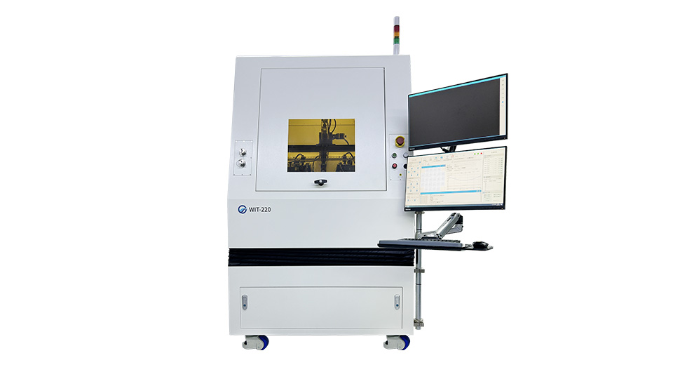
Features
- Automatic calibration with machine vision
- Automatic crimping of probes/probe cards
- Automatic light search
- Support small beam diameter chip testing
- Wafer size 2~12inches, customization upon requests
- Temperature range -20℃ ~ 125℃(wider range upon request)
- Customized functions such as automatic loading and unloading and automatic defect inspection are optional
Application
In OO, OE and other technical testing fields, optical testing is compatible with SMF, Lensed Fiber, FA, etc.. Electrical testing is compatible with probe holders or probe cards, meeting the testing needs of various application scenarios in R&D and mass production.