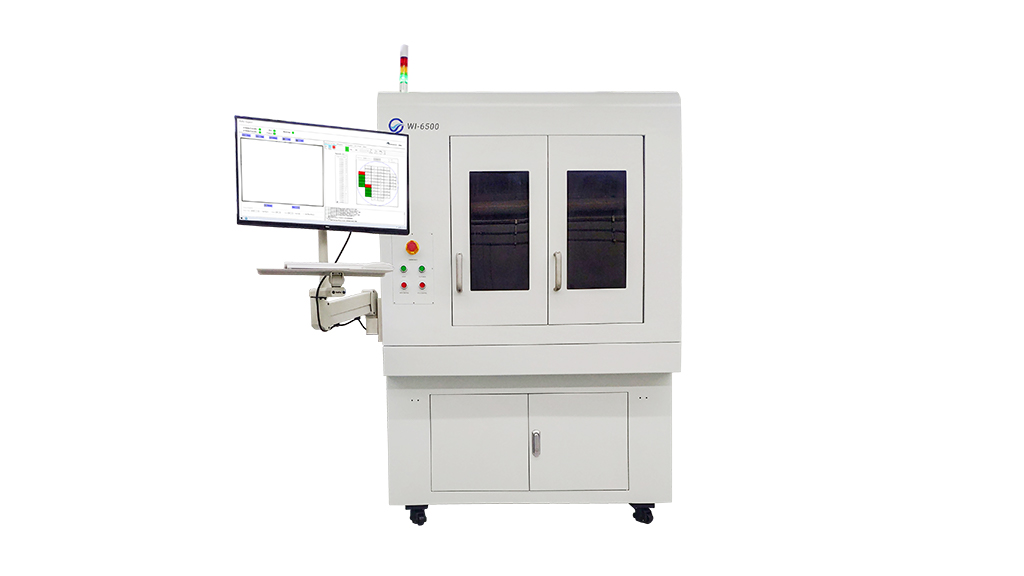
The system supports automatic defect inspection of 25 wafers (1 cassette). It can detect the number and position of wafers in the wafer cassette, quickly detect the defect position, extract the defect image, and fifinally generate the defect map. The results are stored in the system database of the production line for operators and engineers to analyze the defects of the products.
Compared with manual inspection, this system has obvious advantages. It can perform long-term high-precision and high-efficiency inspection with high accuracy, which can greatly improve produc tion efficiency and inspection accuracy, reduce costs and increase efficiency for customers.
Features
- Minimum defect: 0.5μm
- Compatible wafer size: 6 inches, 8 inches, other sizes can be customized
- Automatic loading and unloading, Maximum test volume per batch: 25pcs
- Autofocus and layered focus image capture
- Automatic machine vision inspection
- Defect analysis, generating map report
Application
WI-6500 is suitable for inspecting defects such as stains, scratches, bumps, breaks, discolorations and size errors on wafers.